
Ontime and Stressfree Development withMoney Back Guarantee...
Ontime and Stressfree Development withMoney Back Guarantee...
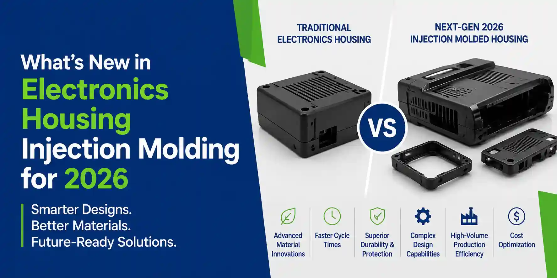
2026 will bring the largest set of changes seen in a decade. Most of these developments originate in core process improvements. Manufacturers now achieve outcomes that were impossible two years ago. The electronics housing injection molding solves long-standing overheating problems.
Faster cycle times are now standard across all high-volume production. This change reduces unit cost with no reduction in finished part quality. Manufacturers now produce thinner walls with no loss of impact strength. The electronics housing injection molding now delivers advanced parts.
Advances in process technology continue to reshape part design and performance. Most developments focus on reducing secondary operations and assembly steps. Manufacturers now achieve outcomes. Most high-volume production now uses electronics housing injection molding for all external components.
This process now produces consistent wearable device cases at high volumes. Tolerances remain stable across production runs of over one million parts. No secondary finishing is required for most consumer-grade applications. The injection molding electronics is the only viable process for these components.
This technology creates integrated gaskets in a single full molding cycle. Two or three materials bond permanently with no risk of delamination over time. This eliminates manual adhesive application from production lines.
This process embeds conductive circuits directly during the molding cycle. No separate circuit mounting or fasteners are required after part ejection. This reduces the total part count for many devices.
Structural foam injection reduces finished part weight. The material retains equal impact and tensile strength to solid resin parts. This allows significant battery size increases with no change to device weight.
Gas assisted molding creates smooth and complex hollow geometries with no sink marks. The process produces consistent wall thickness across large flat surfaces. It eliminates post molding warpage common in thin parts.
Vibration welding now replaces adhesives for permanent assembly. This creates a bond stronger than the base material of both parts. Real time mold monitoring prevents common defects. The electronics injection molding now achieves first pass yield.
|
Smart Materials Used in Electronics Housings |
||
|
Material Type |
Key Property |
Best Application |
|
Graphene-Infused Resin |
High heat dissipation |
Processors & GPU housings |
|
Self-Healing Polymer |
Auto-repairs minor cracks |
Wearable device cases |
|
Conductive Thermoplastic |
Built-in EMI shielding |
Communication devices |
|
Bio-Based Compound |
Sustainable & strong |
Consumer electronics |
|
Phase-Change Material |
Temperature regulation |
Battery enclosures |
|
Anti-Microbial Polymer |
Prevents bacterial growth |
Medical device housings |
2026 design standards have shifted completely to integrated features. Designers now eliminate separate components from the final assembly.
Built in thermal management channels are molded directly into the housing wall. Snap fit assemblies eliminate screws from most consumer devices. These joints maintain clamping force for the full service life of the product.
Integrated cable management pathways remove the need for separate clips and ties. Modular housing sections allow fast repair without full disassembly of the device.
]Ultra thin bezels now reach a consistent thickness under 0.5 millimetre. Textured grips are molded into the surface with no secondary coating. No additional surface treatment is required for scratch resistance.
Wireless charging coil mounting points require no additional adjustment after assembly. Locating pins for all internal components are molded to micron level tolerance.
The electronics plastic injection molding enables all of these design features at volume production. The plastic molding for electronics has removed limits on design geometry.
5G has created the largest single shift in housing requirements for twenty years. Material selection is no longer driven only by strength and flame resistance.
Total heat generation inside modern 5G devices is three times higher than that of 4G equivalents.
The thin housings are required to deliver acceptable signal penetration at operating frequencies. Most manufacturers have reduced nominal wall thickness. The plastic injection molded components for electronics are now specified for these applications.
Miniaturisation continues to accelerate at a consistent rate every twelve months. Requirements that were considered prototype only in 2024 are now standard production. The tool making capability has advanced faster.
The insert molding is now used for small metal components inside devices. Cleanroom molding prevents particle contamination for optical and sensor applications. Optical grade finishes come directly from the mold with no additional polishing required. The injection moulding solutions for electronic components meet these requirements.
Plastic Injection Molds is a specialist manufacturer of precision tooling for electronics. The company holds over fifteen years experience in complex mold design and manufacture. It serves the medical, automotive and consumer electronics sectors globally.
The company operates advanced CAD/CAM design capabilities for prototyping and production. An in house testing lab validates all mold performance before full production release. The facility is located with direct access to all major material suppliers. It operates fully ISO certified quality management systems across all departments.
Engineering support is provided from initial concept through to full volume production. The company also offers full independent consultation services for new product design. It holds particular expertise in micro molding and multi material housings. The electronics housing injection molding is the core focus of every part of the business.
Smart materials and process automation are no longer optional extras. Sustainability requirements now drive most new material selection decisions. Both regulators and brand owners push for lower carbon material options.
Ongoing miniaturization pushes required precision to entirely new limits. Tolerances that were prototype are now standard production requirements. 5G and IoT create unique and unforeseen housing challenges.
We can now hold much tighter tolerances, use new materials that resist static and heat far better, and produce housings that fit perfectly on the first run. There is no reason to accept ill-fitting housings. To discuss your next electronics project, call us at (647) 294-5240 or email info@plasticinjection-molds.com.